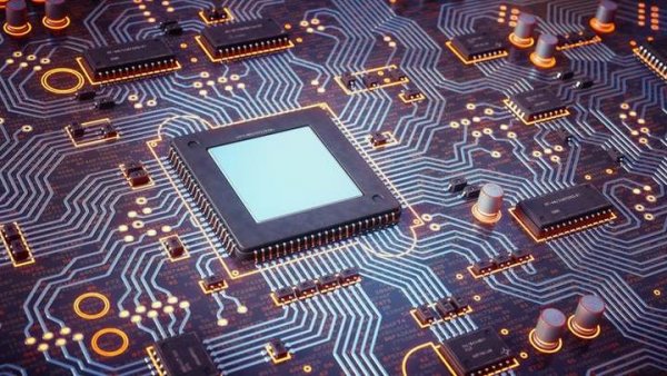
According to foreign media reports, researchers at Cardiff University in the UK have discovered for the first time that the surface of a common semiconductor material has "unstability" that has never been discovered before. This discovery may have a profound impact on the future development of electronic device materials that provide energy for daily life. From smart phones, GPS to satellites and laptops, compound semiconductors are an integral part of such electronic devices.
(Source: Cardiff University)
The new discovery reveals that the surface of a commonly used compound semiconductor material, gallium arsenide (GaA), is not as stable as previously thought.
Using the state-of-the-art equipment of Cardiff University ’s School of Physics and Astronomy and the Composite Semiconductor Research Institute, the team discovered that the atomic structure of gallium arsenide has small instabilities, and these instabilities will appear and disappear once and for all. This is the first time this "meta-stable" phenomenon has been observed on the surface of gallium arsenide.
Co-author of the study, Dr. Juan Pereiro Viterbo of the Cardiff University School of Physics and Astronomy, said: "At present, we do not know whether this phenomenon will affect the growth of semiconductor device structures. It occurs in the growth process of semiconductor devices, and it will have a profound impact. Ultimately, this discovery can help us better understand what is happening on the molecular structure, so that we can develop new materials and structures and reduce the defects of existing composite semiconductors. Develop better electronic products for communication systems, computers, telephones, automobiles, etc. "
The key to this discovery is that new equipment may be created, and such equipment will have new capabilities that did not previously exist.
The laboratories of the School of Physics and Astronomy and the Institute of Composite Semiconductors have a low-energy electron microscope, combined with the use of molecular beam epitaxy machines, and researchers can observe the dynamic changes of the material structure when manufacturing composite semiconductors. Molecular beam epitaxy is a technique used to manufacture or "grow" composite semiconductor devices. Its working principle is to accurately emit extremely hot atomic beams or molecular beams on a substrate. Such molecules fall on the surface of the substrate, condense, and then slowly and systematically accumulate into an ultra-thin layer, eventually forming a complex single crystal structure.
Dr. Viterbo, said: "Although GaAs has been intensively studied during the growth process using low-energy electron microscope, it can be observed that the dynamic situation never observed before." (Author: Yuqiu Yun)
Center Drill Bit is also known as Slocombe Drills, Centre Drills were originally designed to create the countersink required to locate a tailstock centre when turning between centres. They have a point angle of 60° to match the angle of a Tailstock Centre.
A Centre Drill can also be used to provide a start location for a drill when drilling down the centre of a bar held in a Lathe chuck. Centre Drills are short and rigid enough to mark the bar centre without wandering off if they are carefully offered up to a rotating work-piece.


Carbide Center Drills,Hardware Tool Step Drill Bit,Wooden Box Packed Drill,Hss Center Drill Set
Behappy Crafts (suzhou)Co.,Ltd , https://www.jshaoyue.com